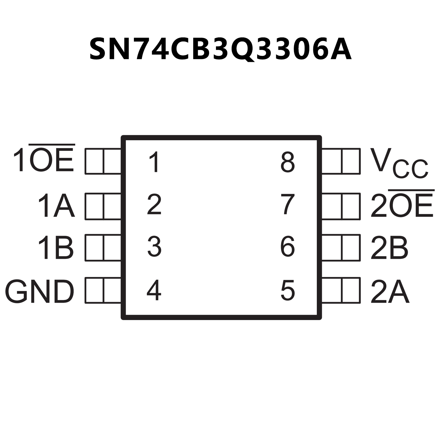


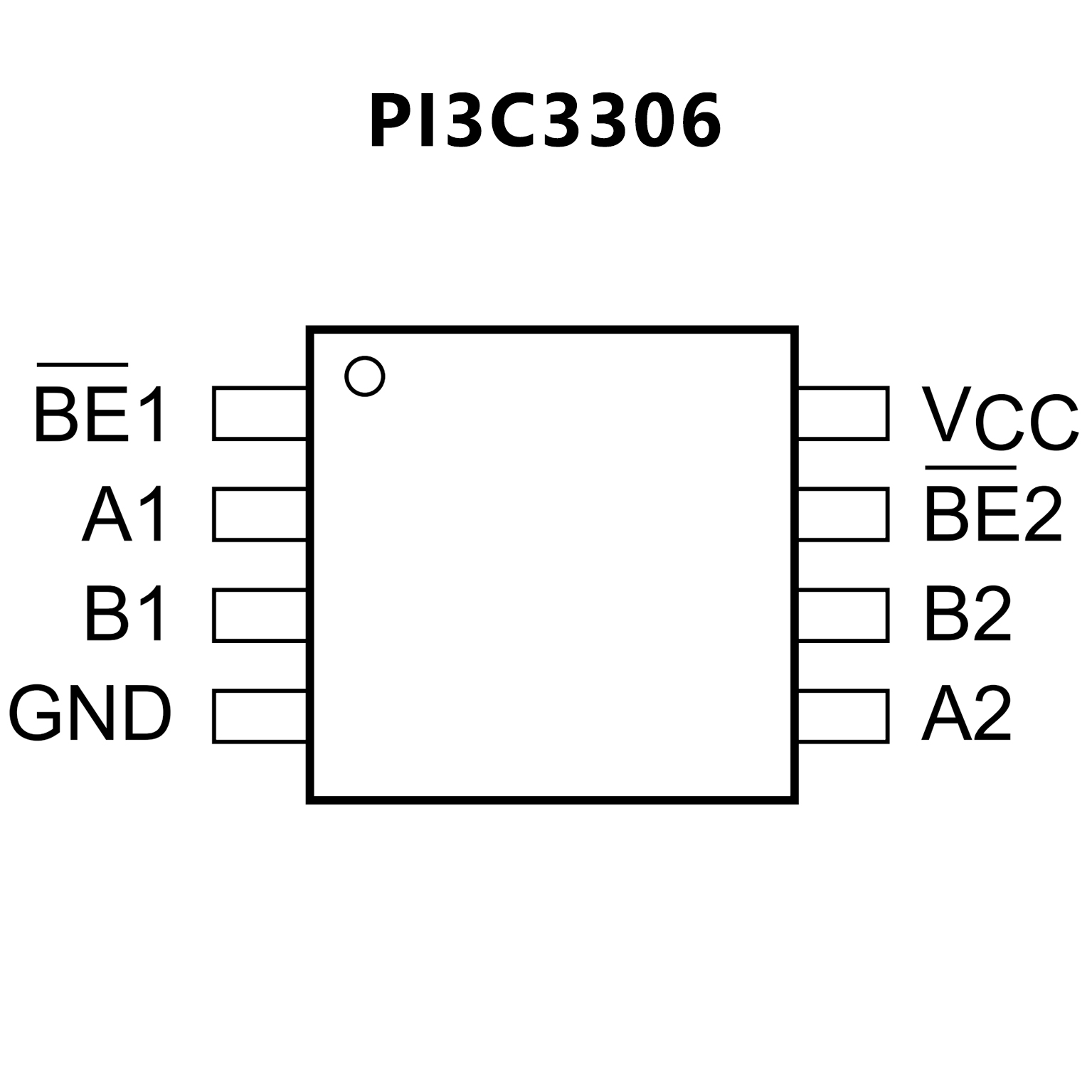
 PI3C3306.pdf
• Near-Zero propagation delay
•5Q switches connect inputs to outputs
• High Bandwidth (>400 MHz)
• Rail-to-Rail,3.3V or 2.5V Switching
• 5V I/O Tolerant
• 2.5V Supply Voltage Operation
•Permits Hot Insertion
• Packaging:
-8-pin 173-mil wide plastic TSSOP
-8-pin 118-mil wide plastic MSOP
• High-Bandwidth Data Path (up to 500 MHz(1)
• 5-V-Tolerant I/Os With Device Powered Up or
Powered Down
• Low and Flat ON-State Resistance (ron)
• Characteristics Over Operating Range (ron = 4 Q Typ)
• Rail-to-Rail Switching on Data I/O Ports
- 0- to 5-V Switching With 3.3-V Vcc
- 0- to 3.3-V Switching With 2.5-V Vcc
• Bidirectional Data Flow With Near-Zero Propagation Delay
• Low Input/Output Capacitance Minimizes
Loading and Signal Distortion (Cio(OFF) = 3.5 pF Typ)
• Fast Switching Frequency (f oE = 20 MHz Max)
• Data and Control Inputs Provide Undershoot
Clamp Diodes
• Low Power Consumption (Icc = 0.25 mA Typ)
• Vcc Operating Range From 2.3 V to 3.6 V
•Data I/Os Support 0- to 5-V Signaling Levels
(0.8 V, 1.2 V, 1.5 V, 1.8 V, 2.5 V, 3.3 V, 5 V)
• Control Inputs Can Be Driven by TTL or 5V/3.3V
CMOS Outputs
• Ioff Supports Partial-Power-Down Mode Operation
• Latch-Up Performance Exceeds 100 mA Per JESD 78,
Class Il
• ESD Performance Tested Per JESD 22
2000-V Human-Body Model (A114-B, Class I)
1000-V Charged-Device Model (C101)
• Supports Both Digital and Analog
• Applications: USB Interface, Differential Signal
Interface, Bus Isolation, Low-Distortion Signal Gating