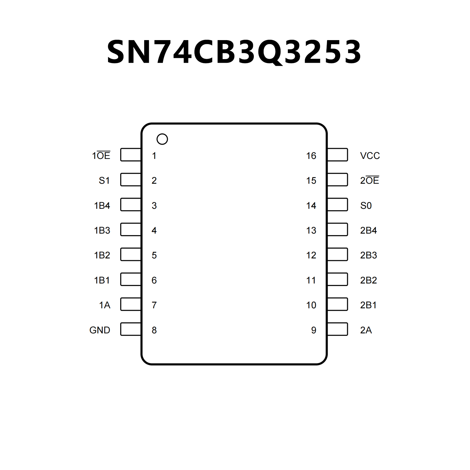


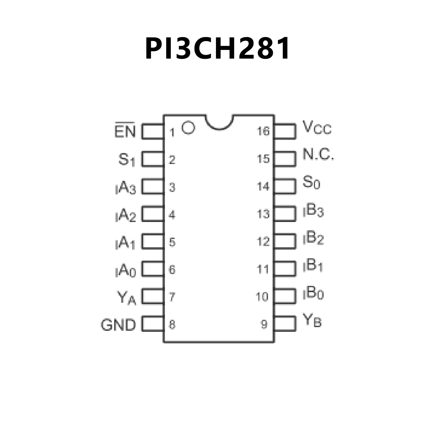
2-Channel 4:1 Mux/DeMux, Enable Low 1.8V/2.5V/3.3V, High-Bandwidth, Hot Plug, PI3CH281 P2P SN74CB3Q3253.
PI3CH281 PI3CH281.pdf
PI3CH281.pdfFEATURES
• Near-Zero propagation delay
• 5-ohm switches connect inputs to outputs
• High signal passing bandwidth (300 MHz)
• Beyond Rail-to-Rail switching
• 0 to 5V switching with 3.3V power supply
• 0 to 3.3V switching with 2.5V power supply
• 5V I/O tolerant with supply in OFF and ON state
• 1.8V,2.5V and 3.3V supply voltage operation
• Hot Insertion Capable
• Industrial Operating Temperature: -40℃ to +85℃
• 8kV ESD Protection (human body model)
• Latch-up Performance: >20OmA per JESD17
• Packaging (Pb-free & Green available):
-16-pin 150-mil wide plastic QSOP (Q)
PIN CONFIGUTION
优势替代
FEATURES
• High-Bandwidth Data Path (Up to 500 MHz)
• 5V Tolerant I/Os With Device Powered Up or Powered Down
• Low and Flat ON-State Resistance (ron) Characteristics
Over Operating Range (ron = 4 Ω Typical)
• Rail-to-Rail Switching on Data I/O Ports
– 0- to 5-V Switching With 3.3-V VCC
– 0- to 3.3-V Switching With 2.5-V VCC
• Bidirectional Data Flow With Near-Zero Propagation Delay
• Low Input/Output Capacitance Minimizes Loading
and Signal Distortion (Cio(OFF) = 3.5 pF Typical)
• Fast Switching Frequency (fOE = 20 MHz Max)
• Data and Control Inputs Provide Undershoot
Clamp Diodes
• Low Power Consumption (ICC = 0.6 mA Typical)
• VCC Operating Range From 2.3 V to 3.6 V
• Data I/Os Support 0- to 5-V Signal Levels (0.8-V,
1.2-V, 1.5-V, 1.8-V, 2.5-V, 3.3-V, 5-V)
• Control Inputs Can be Driven by TTL or 5-V and
3.3-V CMOS Outputs
• Ioff Supports Partial-Power-Down Mode Operation
• Latch-Up Performance Exceeds 100mA Per JESD78, Class II
• ESD Performance Tested Per JESD 22
– 2000-V Human-Body Model (A114-B, Class II)
– 1000-V Charged-Device Model (C101)
• Supports Both Digital and Analog Applications: USB
Interface, Differential Signal Interface Bus Isolation,
Low-Distortion Signal Gating
PIN CONFIGUTION