


8-Channel, Low Noise, Low Power, 24-Bit, Sigma-Delta ADC with PGA and Reference, SGM52421R8 P2P AD7124-8.
SGM52421R8 SGM52421R8.pdf
SGM52421R8.pdfFEATURES
• Power Supply Range: 2.7V to 3.6V and ±1.8V
• 3 Power Modes Available
• Up to 23 Noise Free Bits in Full Power Mode
with Gain = 1
• Rail-to-Rail Analog Inputs Applicable for Gains > 1
• Simultaneous 50Hz/60Hz Rejection at 25SPS
(Single Cycle Settling)
• Crosspoint Multiplexed Analog Inputs
Provide 8 Differential/15 Pseudo Differential Inputs
• Programmable Gain Allows Settings from 1 to 128
• Matched Programmable Excitation Currents Integrated
• Internal Clock Oscillator Included
• On-Chip Bias Voltage Generator Available
• Low-side Power Switch Incorporated
• General-Purpose Outputs Provided
• Multiple Filter Options Offered
• Internal Temperature Sensor for Enhanced Functionality
• Self and System Calibration Capabilities
• Sensor Burnout Detection Enabled
• Automatic Channel Sequencer Simplifying Operations
• Per Channel Configuration Customizable
• Support Independent Interface Power Supply
• 3-Wire or 4-Wire Serial Interface
Compatible with SPI, QSPI, Microwire, and DSP
Equipped with Schmitt Trigger on SCLK
• Operating Temperature Range: -40℃ to +125℃
• Available in a Green TQFN-5×5-32IL Package
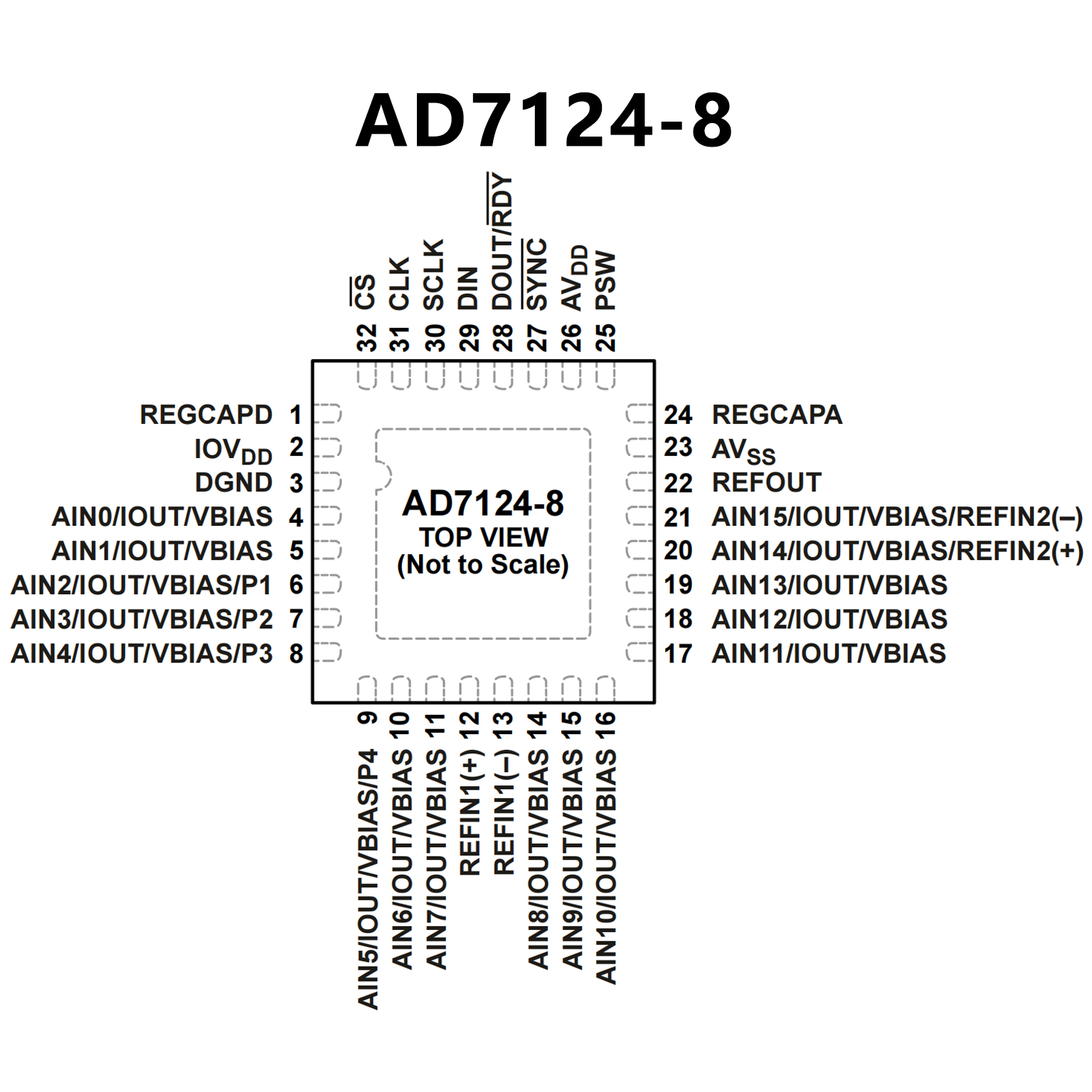
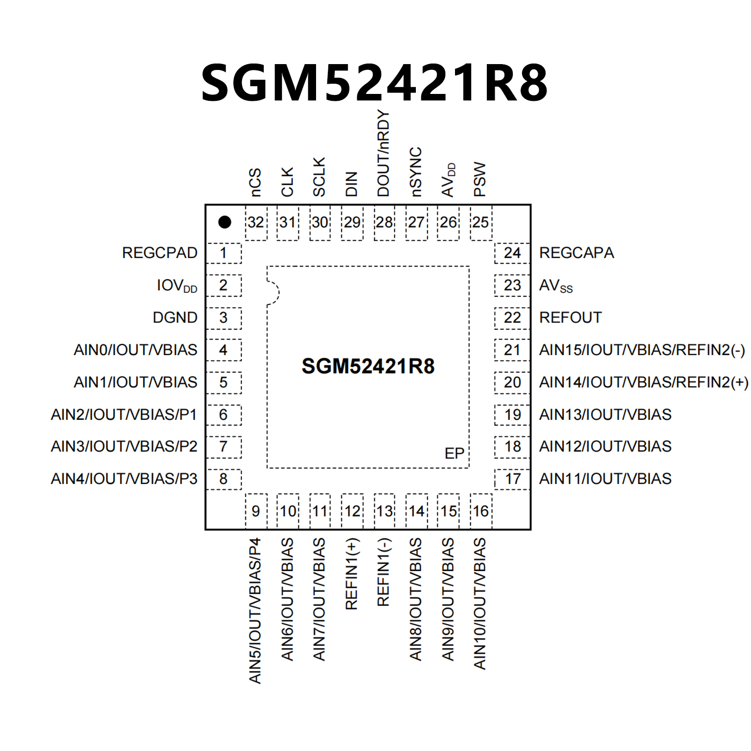
PIN CONFIGUTION
优势替代
FEATURES
• 3 power modes
• RMS noise
Low power: 24 nV rms at 1.17 SPS, gain = 128
(255 µA typical)
Mid power: 20 nV rms at 2.34 SPS, gain = 128
(355 µA typical)
Full power: 23 nV rms at 9.4 SPS, gain = 128
(930 µA typical)
• Up to 22 noise free bits in all power modes (gain = 1)
• Output data rate
Full power: 9.38 SPS to 19,200 SPS
Mid power: 2.34 SPS to 4800 SPS
Low power: 1.17 SPS to 2400 SPS
• Rail-to-rail analog inputs for gains > 1
• Simultaneous 50 Hz/60 Hz rejection at 25 SPS
(single cycle settling)
• Diagnostic functions (which aid safe integrity level
(SIL) certification)
• Crosspoint multiplexed analog inputs
• 8 differential/15 pseudo differential inputs
• Programmable gain (1 to 128)
• Band gap reference with 10 ppm/°C drift maximum (70 µA)
• Matched programmable excitation currents
• Internal clock oscillator
• On-chip bias voltage generator
• Low-side power switch
• General-purpose outputs
• Multiple filter options
• Internal temperature sensor
• Self and system calibration
• Sensor burnout detection
• Automatic channel sequencer
• Per channel configuration
• Power supply: 2.7 V to 3.6 V and ±1.8 V
• Independent interface power supply
• Power-down current: 5 µA maximum
• Temperature range: −40°C to +125°C
• 32-lead LFCSP
• 3-wire or 4-wire serial interface
SPI, QSPI™, MICROWIRE™, and DSP compatible
Schmitt trigger on SCLK
• ESD: 4 kV
• AEC-Q100 qualified for automotive applications
PIN CONFIGUTION